Indian Institute of Science, Samsung join hands for semiconductor R&D
Updated: Feb 09, 2023 04:55:49pm

Indian Institute of Science, Samsung join hands for semiconductor R&D
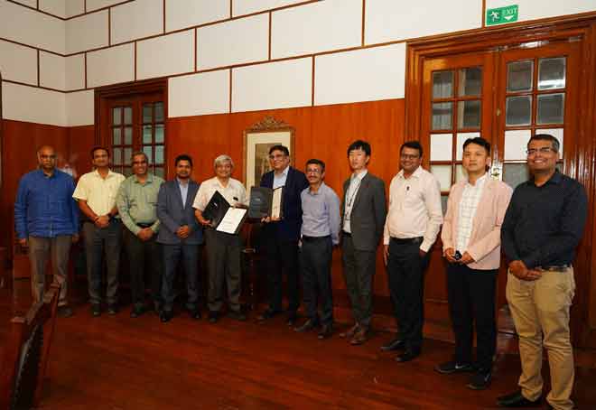
Bengaluru, Feb 9 (KNN) The Samsung Semiconductor India Research (SSIR) is collaborating with the Indian Institute of Science (IISc) to boost research and development in the Indian semiconductor industry.
Under the agreement, IISc and SSIR will work on promoting research and development in protecting semiconductor chips against Electrostatic Discharge (ESD).

ESD is the transfer of electrostatic charge between two bodies. It has become a growing issue in the semiconductor industry as a major cause of destruction for the chips.
“The partnership will help develop solutions, especially to protect ‘ultra-high-speed serial interfaces’ in advanced Integrated Circuits (ICs) and system-on-chip (SoC) products,” IISc said on Wednesday.
ICs and SoCs, both essential to all systems, are very sensitive to ESD failures, especially those developed using advanced nanoscale CMOS (Complementary Metal Oxide Semiconductor) technologies. ESD failures contribute to most of the IC chip failures and field returns.
The partnership is significant considering that R&D in ESD technology for highly reliable interfaces and SoCs that operate at low power and high speed is integral to innovation in semiconductors.
“We have been collaborating extensively with semiconductor industries worldwide on advanced Nano electronics technologies, including solutions to ESD reliability threats to advanced SoCs,” Mayank Shrivastava, professor at the IISc Department of Electronic Systems Engineering.
Shrivastava said, “We have carried out both fundamental and applied research on ESD protection devices, with a strong emphasis on creating practical solutions for the semiconductor industry in a range of technology nodes.” (KNN Bureau)


 Loading...
