80% of Centre’s $10 Billion Semiconductor Production Funds Remains Untapped
Updated: Nov 08, 2023 04:25:42pm

80% of Centre’s $10 Billion Semiconductor Production Funds Remains Untapped
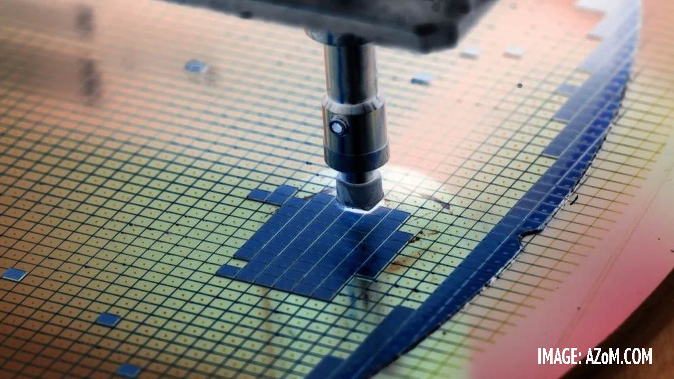
New Delhi, Nov 8 (KNN) Around 80 per cent of the funds allocated by the Union government for the production of semiconductors under the PLI scheme remains untapped, reported the Hindu citing top Industry Ministry official on Tuesday.
Around USD 8 billion of the USD 10 billion allocated under the PLI scheme is unused.
Speaking at the India-Korea Business Partnership Forum hosted by the Confederation of Indian Industry and the Korea International Trade Association, Rajesh Kumar Singh, Department for Promotion of Industry and Internal Trade Secretary urged Korean investors, who have invested USD 5.6 billion in India since April 2000, to use the semiconductor PLI along with upcoming opportunities for investments in battery storage solutions.
Singh said that India and Korea must aim to enhance bilateral trade to USD 50 billion by 2030.
“India is trying to create a transition to a much stronger manufacturing base through schemes like the PLI under which over USD 26 billion is being provided as incentive in 14 sectors of the economy. In high tech areas like the Semiconductor Mission, we are also providing an incentive of over USD 10 billion to encourage semiconductor makers to manufacture in India. There are opportunities for Korean companies, where almost USD 8 billion out of that USD 10 billion remain unsubscribed,” he said.
He added, “We also have an important bid opening soon for over 20 gigawatt hours of storage and mobility battery capacity in India. That’s another area where we hope Korean companies take advantage of these opportunities.”
“I take note of the suggestion that we must upgrade and enhance our CEPA (Comprehensive Economic Partnership Agreement) to further strengthen this relationship,” Singh said.
(KNN Bureau)


 Loading...


