Centre Notifies Rs 1.27 Lakh Crore Semicon 2.0 With Expanded Support For Chip Startups, MSMEs
Updated: Sep 01, 2026 02:53:46pm

Centre Notifies Rs 1.27 Lakh Crore Semicon 2.0 With Expanded Support For Chip Startups, MSMEs
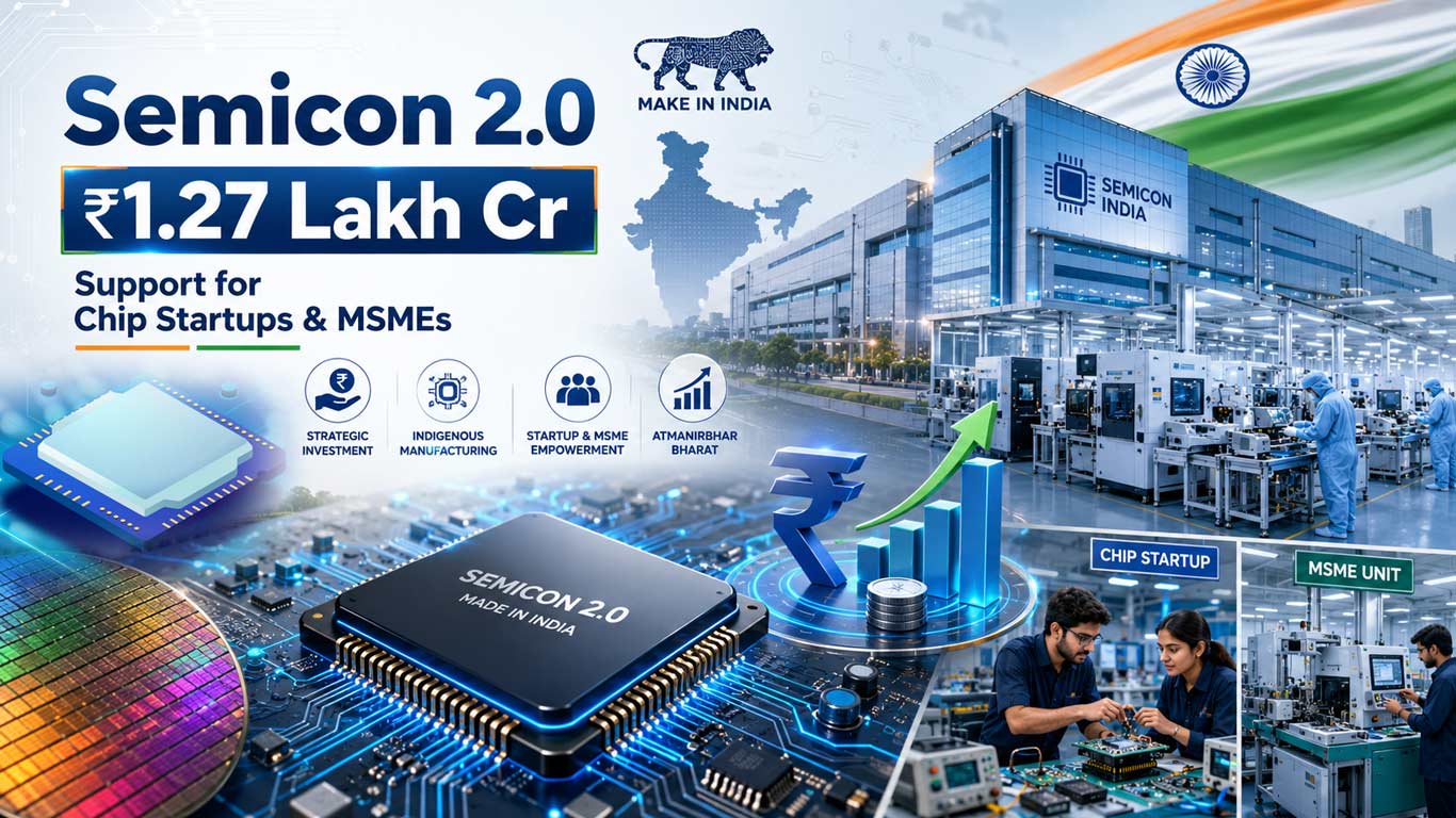
New Delhi, Sept 1 (KNN) The Central government has formally notified Semicon 2.0, a Rs 1,27,500-crore programme to expand India’s semiconductor ecosystem across design, intellectual property, equipment, materials, advanced packaging, R&D and talent development.
Following the Union Cabinet’s July 15 approval, MeitY has outlined incentives across six pillars and 10 categories. IT Secretary S Krishnan said the scheme will strengthen domestic capabilities and build a globally competitive industry.
Unlike the first phase, Semicon 2.0 expands participation to chip-design startups and MSMEs, fabs, packaging firms, equipment and materials manufacturers, research organisations and training institutions, reported Business Today.
Chip Design, Fabs Get Targeted Support
Indian companies owned or controlled by Indian citizens or Overseas Citizens of India (OCIs), including startups and MSMEs, will be eligible for commercial chip-design support.
Startups can access seed funding, equity co-investment and other assistance, while larger companies may receive royalty financing or equity co-investment.
300-mm Wafer Fabs To Receive 40 percent Capex Support
For 300-mm silicon wafer fabs, the government will provide 40 percent of eligible capex, down from 50 percent under the first phase.
Applicants must have a minimum capacity of 40,000 wafer starts per month, use licensed production-grade technology, invest at least Rs 20,000 crore, and report Rs 7,500 crore revenue in at least one of the previous three financial years.
Compound Semiconductor Fabs Get 35 percent Support
Compound semiconductor, photonics, sensor/MEMS and discrete semiconductor fabs will receive 35 percent capex support, with projects requiring at least Rs 500 crore investment, Rs 200 crore revenue and 500 wafer starts per month.
Display fabs, including OLED, Micro LED and LCD, will also receive 35 percent support, subject to technology-specific conditions.
Advanced ATMP/OSAT facilities will get 35 percent capex support, while conventional packaging projects will receive 25 percent, with applicants requiring at least Rs 1,000 crore capex and Rs 200 crore revenue.
Support Extended To Semiconductor Equipment And Materials
The scheme covers semiconductor equipment, sub-assemblies, components and materials. Equipment projects require at least Rs 300 crore capex and Rs 120 crore revenue, while semiconductor-grade raw-material projects need Rs 50 crore capex and Rs 20 crore revenue.
Test and characterisation facilities require Rs 100 crore capex and Rs 40 crore revenue.
Equipment manufacturers will also receive a 10 percent, 8 percent, 6 percent, 4 percent or 2 percent PLI on domestic bills of materials for five years from FY29, capped at 50 percent of eligible capex.
Startups, MSMEs To Get Design And R&D Support
Eligible chip-design startups and MSMEs can access the Design Infrastructure Support framework, including national electronic design automation (EDA) tools and multi-project wafer fabrication services.
They can also receive seed funding of up to Rs 15 crore, subject to a cap of 50 percent of the project cost.
Up To 75 percent Support For Semiconductor R&D
Semicon 2.0 offers up to 75 percent support for advanced semiconductor R&D and talent development, subject to project-specific conditions.
Under the first phase, the government approved 12 semiconductor projects across six states, with commercial production already underway at Micron’s ATMP facility, Kaynes Semicon and CG Semi’s OSAT facility, according to the government.
(KNN Bureau)









 Loading...